
lifespan of a high density interconnect
The lifespan of a high density interconnect depends on the design rules and fabrication process. In order to maximize the lifespan of your HDI PCB, make sure to avoid components that have short lead lengths or are susceptible to bending. Additionally, it’s important to minimize component clustering and to plan out the layout of your circuit board. In addition, it’s necessary to choose the right material for your PCB, as it will impact reliability and cost. In general, FR4 is the best material choice because it offers excellent electrical properties. It’s also a good idea to choose a high-density PCB with a thick copper foil, as it will increase electrical performance and reduce the number of vias.
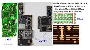
Unlike traditional PCBs, high density interconnect PCBs use microvias to connect layers of the board. Using this technology, engineers can route signals more easily and more efficiently. This leads to a smaller footprint, lower layer count and lower manufacturing costs. Additionally, the microvias used in HDI PCBs can withstand higher frequencies than conventional PCBs.
In terms of material choices, high-density interconnect PCBs are available in a variety of materials and thicknesses. They can range from 0.2mm to 10mm, allowing them to fit into different devices and meet their performance needs. In addition, they can incorporate different surface finishes, including ENIG, HASL and immersion tin.
What is the lifespan of a high density interconnect?
Another advantage of HDI PCBs is that they are very compact, allowing them to fit into small spaces and making them ideal for portable electronic devices. This is especially helpful for medical and industrial equipment. For example, advanced electronic medical devices such as monitors and surgical tools may incorporate HDI technology. Similarly, IoT sensors that are used in warehouses and other industrial settings to track inventory and provide data analytics often incorporate HDI technology.
HDI PCBs can also be made with multiple laminations to create complex designs and prevent signal interference. They can contain buried and blind vias, which are miniaturized holes that allow traces to be routed in confined spaces. This feature allows engineers to add more features to a device while reducing its size and weight.
Additionally, HDI PCBs have fewer holes and shorter traces, which makes them more reliable. This is because there is less distance for the heat to travel through the board. It also undergoes less stress during operation and assembly, which can extend its life.
HDI technology is vital for the future of electronic devices, and it will continue to play a role in the development of new technologies. Its ability to enable more advanced components to be packed into a smaller package without sacrificing performance has made it an essential part of modern technology. As the world becomes increasingly dependent on digital devices, the need for high-density interconnects will continue to grow.


+ There are no comments
Add yours