
Blind Vias Over Buried Vias
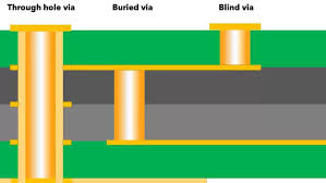
When designing a printed circuit board it’s not always possible to fit all of the necessary connections on one layer. In those instances, vias are used to make the connection between layers. Vias are barrel shaped vertical conductive holes that connect multiple layers on a PCB and can be either blind or buried.
There are several different types of blind via including photo-defined, controlled depth, and sequential laminate blind. The most common are through hole and buried vias. Buried vias are created by drilling a hole in one inner layer and then copper plating it to make it conductive. This is done before the rest of the stack up is laminated and pressed together. This allows the fabricator to use a sequential process and reduces manufacturing costs.
Using vias can help to reduce weight, increase circuitry density, improve EMC, and help to shorten signal timing. They are also very important when working with HDI technology. HDI PCBs (High-density interconnect printed circuit boards) are becoming increasingly popular in a variety of devices from laptops to watches and cellphones due to their ability to pack more circuitry into a smaller space. These benefits lead to lower power consumption, shorter development time, and higher functionality.
In What Scenarios Would You Choose Blind Vias Over Buried Vias?
Blind vias are very useful when you want to connect the top and inner layers of the board but don’t want them to touch each other. These vias are not visible from the outside of the board and are usually surrounded by other copper pads. Using blind vias can also reduce the number of layers needed in your board.
The downside of these type of vias is that they can be more difficult to design than buried vias and can also be more susceptible to defects during the manufacturing process. These issues can include signal distortion or degradation and poor connection. Having a good understanding of the PCB fabrication process can help to mitigate these issues.
Both buried and blind vias add cost to the manufacturing of a board as they require extra steps and testing compared to the standard through hole. This can be as simple as incorporating them in the right spot on the board design or as complex as choosing the correct drill depth and filling the hole with the appropriate conductive material.
The best way to ensure the quality of your blind and buried vias is to work with a PCB manufacturer that is experienced in manufacturing high-density circuit boards. Contact us today for more information about our services and to get a quote for your next project. We offer fast and free quotes. Our expert engineers can look at your engineering requirements, space needs and functionality of your product to determine the best ways to use buried or blind vias in your board. We are dedicated to providing you with the highest quality products and excellent customer service.


+ There are no comments
Add yours