
PCB HDI Improve Signal Integrity
In electronic circuits, signal integrity refers to the quality of signals that travel through a PCB. The higher the signal integrity, the better the performance of the circuit. Achieving high signal integrity is essential for high-speed digital and RF applications. Achieving this requires high-speed traces with controlled impedance and differential pair routing. To minimize signal degradation, engineers must use proper design techniques and follow strict guidelines.
High-density interconnect or pcb hdi utilize smaller traces and spaces, which allows manufacturers to pack more components on the board with higher density. Moreover, the use of blind and buried vias further improves signal integrity by reducing transmission delays. As a result, high-speed signals can be transmitted with more accuracy and speed.
This improved signal integrity is crucial for enabling faster and more reliable devices, such as 5G mobile communications, networking equipment, medical devices, IoT, LiDAR systems, intelligent munitions, and autonomous vehicles. The higher signal integrity of HDI PCBs also contributes to lower power consumption, which makes them more energy-efficient and environmentally friendly.
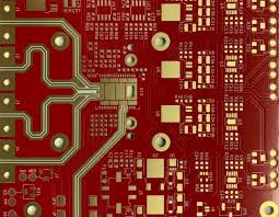
How Does PCB HDI Improve Signal Integrity?
Sequential lamination is a key aspect of the HDI PCB manufacturing process. During this process, thin layers of thin dielectrics are assembled in sequences to build up the PCB. This construction also includes microvias that connect inner layers to the outside of the PCB. These microvias are drilled using laser technology, which helps ensure their reliability.
The use of sequential build-up also helps protect the PCB from thermal shocks, which can cause degradation and deformation over time. This provides superior reliability, making HDI PCBs a viable solution for use in harsh environments.
Uneven line impedance is a major source of signal degradation. This issue can occur when the signal travels through different layers of the PCB or unequal trace lengths. It can lead to waveform skewing and timing misalignment, especially in signals that carry data.
Another major factor that can affect signal integrity is poor copper foil selection. The thickness of the copper foil and the metallization processes used are critical to the performance of a PCB. Insufficient copper may decrease the conductivity of the PCB, leading to higher temperatures and potential failures. Fortunately, PCB manufacturers can improve the signal integrity of their boards by selecting the appropriate copper foils for each application.
The use of high-quality PCB materials is essential for achieving high-density circuit boards that offer exceptional signal integrity and other important qualities. High-density PCBs are more difficult to route than their traditional counterparts, and engineers must carefully plan their designs with high-speed signals in mind. Using proper layer stackups, signal-routing guidelines, and specialized tools for signal-integrity analysis can help designers achieve the best results. These tools can simulate the behavior of high-speed signals in a PCB, including their susceptibility to crosstalk and EMI. They can also provide real-time DRC (design rule checking) to help ensure that the design adheres to the highest standards of signal integrity. In addition, advanced PCB software such as Altium Designer and Cadence Allegro, can support the design of high-speed signals by providing features such as controlled-impedance traces and differential pair routing.


+ There are no comments
Add yours